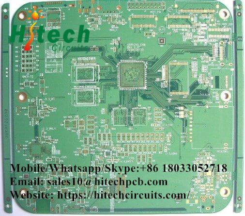
HDI PCB is the abbreviation of High Density Interconnect PCB or High Density PCB. HDI PCB is defined as a printed circuit board with higher wiring density per unit area than traditional PCB. Hitech Circuits Co., Limited is a professional High Density Interconnect PCB, HDI PCB board manufacturer, supplier and design company from China, if you are looking for a reliable High Density Interconnect PCB board partner from China, please feel free to contact sales@hitechcircuits.com .
What is High Density Interconnection PCB Board
HDI is the abbreviation of High Density Interconnection, which is a technology for producing printed circuit boards. High-density interconnection PCB boards are circuit boards with relatively high line distribution density using micro blind and buried via technology.
HDI includes the use of fine features or signal routing and space of 0.003 inches (75μm) or less and laser drilling blind or buried via technology. Microvias allow the use of micro interconnects from one layer to another within the PCB, using smaller pad diameters to produce additional wiring density or reduce the overall size.
HDI PCB boards are compact products designed for small-volume users.
Advantages of High-density Interconnection PCB Boards
PCB costs can be reduced: When the density of the PCB increases to more than eight layers, the cost of HDI manufacturing will be lower than the traditional complex lamination process.
Increase circuit density: better interconnectivity between traditional circuit boards and parts
Conducive to the use of advanced construction technology
Better electrical performance and signal accuracy
Better reliability
Can improve thermal performance
Can improve radio frequency interference (RFI), electromagnetic interference (EMI), electrostatic discharge (ESD)
Improve design efficiency
Disadvantages of high-density interconnected PCB boards
NDI impedance values are concentrated on pattern transfer (pattern complexity) and pattern electroplating process.
Abnormal quantity and quality, especially the etching speed of the high-density circuit part of the HDI PCB board is slower than the isolation line, causing excessive etching of the isolation line.
When the entire HDI board is electroplated and etched, a large area of copper on the PCB circuit board will be etched away, increasing production costs. At the same time, a large amount of copper ions enter the waste liquid after etching, causing environmental pollution and difficulty in recycling.
High-density interconnected PCB board Vs ordinary PCB board
Ordinary PCB boards are mainly FR-4, which are pressed together with epoxy resin and electronic-grade glass cloth. Traditional HDI PCB boards generally use backing copper foil on the outer surface. Since laser drilling cannot penetrate the glass cloth, copper foil without glass fiber backing is generally used. But the current high-energy laser drilling machine can penetrate 1180 glass cloth. This is no different from ordinary PCB board materials.
Application of high-density interconnect PCB boards
While electronic design continues to improve the performance of the whole machine, researchers are also working hard to reduce its size. In small portable products from mobile phones to smart weapons, "small" is an eternal pursuit. High-density interconnect (HDI PCB) technology can make the terminal product design more compact while meeting higher electronic performance and efficiency standards. HDI PCB boards are widely used in digital products such as mobile phones, digital cameras, MP3, MP4, laptops, automotive electronics, IC substrates, etc., among which mobile phones are the most widely used.
High-density PCBs are widely used in the following applications and industries:
Mobile phones
GPS
Telecommunications
Semiconductors
Automobiles
Military
Medical
Instruments and meters
Laptops
IC substrates
Healthcare
Mobile/Whatsapp/Skype:+86 18033052718
Email: sales10@hitechpcb.com
Website: https://hitechcircuits.com/pcb-products/high-density-interconnect-pcb/

