
Basics of PCB Stack-up
A PCB stack-up is the arrangement of conductive and insulating layers in a multilayer PCB, crucial for electrical performance, mechanical strength, and manufacturability. Proper stack-up design optimizes signal integrity, minimizes electromagnetic interference (EMI), and ensures reliability.
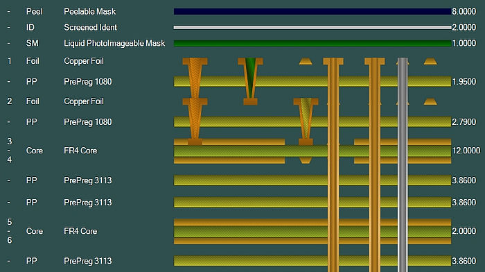
Primary Components:
Core Material: The core is a rigid, insulating substrate (e.g., fiberglass-reinforced epoxy laminate like FR4) providing mechanical strength.
Prepreg: Fiberglass sheets impregnated with resin, bonding core, and conductive layers when heated and pressed.
Copper Layers: Conductive layers forming the circuitry, etched to create desired patterns.
Solder Mask: A protective layer insulating copper traces and preventing solder bridging during assembly.
Silkscreen: Printed text and symbols on top of the solder mask, providing information about component placement. Effective stack-up design involves considering layer count, signal and power plane arrangement, layer thickness, and material types. Balancing electrical performance with manufacturability ensures the PCB meets specifications cost-effectively.
Types of Multilayer PCB Stack-ups
Multilayer PCBs come in various configurations tailored to specific applications and performance requirements:
Standard Multilayer Stack-up:
Configuration: Symmetrical arrangement of signal and ground/power layers.
Applications: General-purpose electronics (consumer devices, industrial controls).
Benefits: Balanced performance and cost, suitable for various applications.
High-Density Interconnect (HDI) Stack-up:
Configuration: Finer lines, smaller vias, higher layer counts, using micro vias and buried/blind vias.
Applications: Compact devices (smartphones, tablets, wearables).
Benefits: High component density, reduced signal paths, improved signal integrity.
Flex and Rigid-Flex Stack-up:
Configuration: Combines rigid and flexible substrates (e.g., polyimide) within a single PCB.
Applications: Flexible form factors (medical devices, aerospace, automotive electronics).
Benefits: Mechanical flexibility, reduced weight, adaptability to unconventional shapes.
Selecting the appropriate stack-up type depends on size, weight, electrical performance, and environmental conditions. Designers must evaluate these factors for optimal configuration.
Design Considerations for Multilayer PCBs
Designing a multilayer PCB requires careful consideration to ensure optimal performance, reliability, and manufacturability:
Signal Integrity:
Definition: Quality of electrical signals through the PCB, affected by crosstalk, reflections, and EMI.
Considerations: Proper stack-up, controlled impedance, careful high-speed signal routing, and ground planes to minimize noise.
Power Integrity:
Definition: Maintaining stable, noise-free power distribution.
Considerations: Minimize voltage drops, ensure even power distribution, and use decoupling capacitors to filter noise and stabilize power.
Thermal Management:
Definition: Controlling PCB temperature to prevent overheating and ensure reliability.
Considerations: Use thermal vias, heat sinks, and appropriate materials to dissipate heat from high-power components.
Material Selection:
Definition: Choosing materials affecting electrical and mechanical properties.
Considerations: Use FR4, polyimide, and high-frequency laminates, considering dielectric constant, loss tangent, and thermal conductivity based on application needs.
Layer Count and Configuration:
Definition: Determining the complexity and capabilities of the PCB.
Considerations: More layers allow routing flexibility and improved performance but increase cost and manufacturing complexity.
Via Types and Placement:
Definition: Holes connecting different PCB layers, including through-hole, blind, buried, and microvias.
Considerations: Impact on signal integrity, manufacturability, and cost. Advanced processes are required for micro vias and buried/blind vias.
Considering these factors during design helps create multilayer PCBs that meet specifications, are cost-effective, and are reliable. Collaboration with PCB manufacturers can optimize the production design, ensuring the final product meets all requirements.
Hitech Circuits is a wоrld-lеаding PCB Manufacturing & PCB Assembly company with more than 20 years experience in the electronics manufacturing industry. We focus on PCB Design, PCB Layout, Circuit board fabrication, Turnkey PCB assembly, and electronic parts sourcing services. If you have any requirements related to electronics, please feel free to contact sales3@hitechpcb.com For more information, please visit our website https://www.hitechpcba.com/