
What is Flex PCB?
Flexible printed circuits, also known as flex circuits, are sometimes regarded as a printed circuit board (PCB) that can bend, when in reality there are significant differences between PCB’s and flex circuits when it comes to design, fabrication and functionality. One common mistake that designers make is to design a flexible circuit using the same rules as a PCB. Flex PCB require a unique set-up and have their own set of design rules that the Hitechpcb team has termed “flex-izing” and have worked hard to perfect over the last many years.
Flexible PCB, which also called Flex PCB, Flexible circuit board or flex circuit, it consists of PI base material, adhesive layer, copper layer, coverlay and sometimes with stiffeners. Flexible PCBs are now being used widely to replace traditional FR4 PCB in various different applications due to the benefits from flex PCB specially. Although more expensive than a normal rigid PCB, the right design in the right application could save weight and time in assembly, coupled with the reliability which makes flexible circuit board a worthwhile consideration.
A flexible printed circuit consists of a metallic layer of traces, usually copper, bonded to a dielectric layer, usually polyimide. Thickness of the metal layer can be very thin (<.0001″) to very thick (> .010″) and the dielectric thickness can vary from .0005″ to .010″. Often an adhesive is used to bond the metal to the substrate, but other types of bonding such as vapor deposition can be used to attach the metal.

How to calculate your flex pcb bend radius?
Because copper tends to readily oxidize, the exposed surfaces are often covered with a protective layer, gold or solder are the two most common materials because of their conductivity and environmental durability. For non-contact areas a dielectric material is used to protect the circuitry from oxidation or electrical shorting.
The number of material combinations that could go into a flexible printed circuit are nearly endless; current, capacitance, chemical and mechanical resistance, temperature extremes and type of flexing are just some of the criteria that impacts the material selections that best meet the functional needs. An experienced Hitechpcb design engineer takes the critical requirements into consideration when designing a circuit to meet your needs.
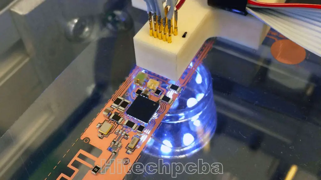
Flexible printed circuit boards (FPC) has become a common component of electronic products due to its lightness and flexibility performance. It is widely used in smart terminal, wearable electronics, consumer, automotive, industrial and medical fields. The miniaturization and integrated function of electronics product development is driving FPC to fine line and multilayer design.
What is Multilayer flex PCB?
This type of flexible printed wiring boards are multilayered (with three or more conductor layers) and require plated-through holes. We could use through vias, buried vias and blind vias.
A multi layer flex circuit combine several single-sided or double-sided circuits with complex interconnections, shielding and/or surface mounted technologies in a multi layer design. The multi layers may or may not be continuously laminated together throughout the production process. If your design needs require maximum flexibility, continuous lamination may not be appropriate. Multi layer circuits are an effective solution when confronted with design challenges such as: unavoidable crossovers, specific impedance requirements, elimination of crosstalk, additional shielding and high component density. You can also link here to learn more about flex pcb bending radius.
Benefits to Flex PCB including:
Assembly Error Reduction
Decreased Assembly Time and Costs
Design Freedom
Flexibility during Installation
High Density Applications
Improved Airflow
Increased Heat Dissipation
Increased System Reliability
Point-to-Point Wire Replacement
Reliability and Durability
Repeatable Routings
Simplified Circuit Geometry
Package Size and Weight Reduction
Flex PCB Static Application
An application where flexible circuits are flexed only to install the circuit and fit it into its application (also known as flex-to-fit or flex-to-install). A static application will typically be made using the less expensive Electro Deposited (ED) copper.
Flex PCB Dynamic Flexing Applications
A situation where the flexible circuit itself is dynamically (repeatedly) flexed during the actual use of the final product. Common examples include flip-type cell phones, laptops, printer heads and robotic arms. A dynamic application will require the use of Rolled Annealed (RA) copper.
High Density Flex PCB Applications
Flexible circuits allow for minutely narrow lines giving way to high density device population. Denser device populations and lighter conductors can be designed into a product, freeing space for additional product features.
With a large number of investments on the facilities of flexible printed circuit board and continuously innovating the flexible circuit board manufacturing technology, Hitech Circuits is able to manufacture flexible PCBs with a great variety of technologies, from simple single sided flex PCB, double sided flex PCB to complex multilayer flexible PCB, Rigid flex pcb and support prototype FPC with laser cutting & flying probe test to mass production with toolings.
Multilayer flex PCB bookbinding
Circuit bookbinding is one of the best practices employed by Hitechpcb engineers for creating stacked PCBs. For flex PCBs, we offered a 12 layer flex PCB board with bookbinding. An additional small length is added to the circuit, making it move in an outward direction from the bend radius. There are copper traces placed at right angles to the bend. This helps restrict the circuit bend in one direction.
https://twitter.com/Roger_PCB_PCBA
https://www.facebook.com/luo.roger.1675/
https://www.instagram.com/roger_hitechpcb_pcba/
https://www.hitechpcba.com
https://www.hitechcircuits.com
https://www.htmpcb.com
WhatsApp:+8618118703950
For more,please contact sales1@hitechpcb.com