
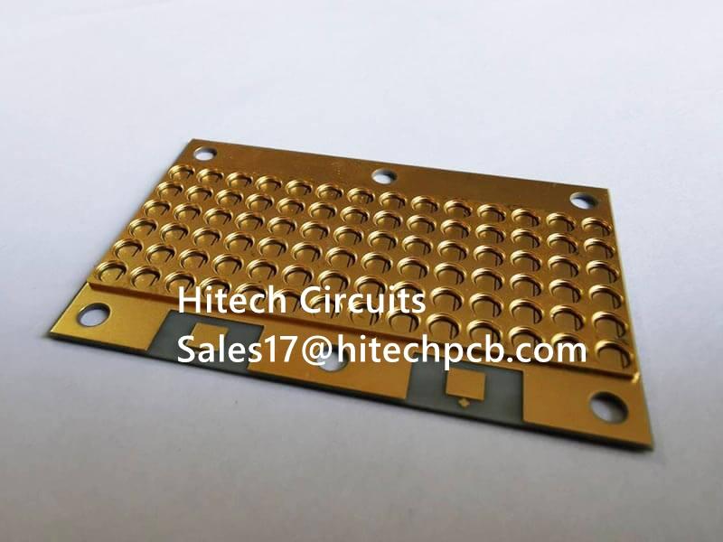
Ceramic Printed Circuit Boards (PCBs) are advanced circuit boards that offer superior performance and reliability, especially in demanding high-performance electronic applications. Unlike conventional circuit boards made from organic materials such as fiberglass or epoxy, ceramic PCBs are manufactured using ceramic materials, which gives them unique properties and features. These boards are designed to excel where high thermal conductivity, excellent electrical performance at high frequencies, and robustness in harsh environments are critical.
Comprehensive Introduction to Ceramic PCBs
The foundation of a ceramic circuit board lies in its ceramic substrate, which has many advantages that distinguish it from conventional circuit boards. One of its outstanding features is its excellent thermal conductivity, which enables it to efficiently dissipate the heat generated by components. This makes ceramic PCBs the first choice for applications that generate large amounts of heat and require efficient thermal management.
The excellent electrical properties of ceramic materials, especially at high frequencies, make ceramic PCBs particularly suitable for radio frequency (RF) and microwave applications. These boards maintain signal integrity and minimize signal loss, making them indispensable in industries such as telecommunications, aerospace and satellite communications.
In addition, ceramic PCBs have impressive mechanical strength and durability, allowing them to withstand challenging mechanical stresses and vibrations. Their chemical resistance and ability to withstand harsh environments make them ideal for applications that require exposure to corrosive substances.
Advances in ceramic PCB manufacturing:
-Ceramic Material Selection: The selection of ceramic materials is critical in defining the characteristics of a PCB. Advances in materials science have given rise to a wider range of ceramics with customized thermal, electrical and mechanical properties that can be precisely tailored to the application requirements.
-Multilayer integration: Ceramic printed circuit boards are often constructed with multiple layers to accommodate complex circuit designs. Innovations in layer stacking, through-hole technology and precise alignment have enabled the creation of high-density, multilayer ceramic circuit boards that support complex circuits in compact form factors.
-Miniaturization technology: State-of-the-art manufacturing processes have unlocked the potential for finer alignments and smaller components to increase the miniaturization of electronic devices. This is especially valuable in applications requiring compactness and high functionality.
-Thick film and thin film technologies: Thick film and thin film deposition technologies allow the precise application of conductive and insulating layers to ceramic substrates. These technologies enable the creation of high-performance circuits with optimized electrical characteristics.
What types of ceramic PCBs are available?
Ceramic Printed Circuit Boards (PCBs) come in a variety of types and configurations, each designed to meet specific application and performance requirements. Here are some common types of ceramic PCBs:
-Single Layer Ceramic PCB: These are basic ceramic PCBs with a single conductive layer on a ceramic substrate. They are typically used for simple applications that require high thermal conductivity but not complex circuitry.
-Multilayer Ceramic PCBs: These PCBs consist of a multilayer ceramic substrate with conductive traces and vias connecting the different layers. Multilayer ceramic PCBs are suitable for complex circuit designs, high-density interconnects, and applications requiring signal integrity.
-Thick Film Ceramic PCBs: In this type, thick film technology is used to create conductive and resistive traces on ceramic substrates. Thick film ceramic PCBs are known for their durability, making them suitable for applications in harsh environments such as automotive and industrial environments.
-Thin Film Ceramic PCBs: Thin film technology involves depositing thin layers of conductive and insulating materials onto ceramic substrates. Thin-film ceramic PCBs have precise electrical characteristics and are typically used in high-frequency applications such as RF and microwave equipment.
-Hybrid Ceramic PCBs: These PCBs combine ceramic materials with other materials such as organic substrates or metal cores. This hybrid approach allows engineers to balance the benefits of ceramics with those of other materials, such as cost-effectiveness or specific thermal properties.
-Aluminum Oxide (Al2O3) Ceramic PCBs: Aluminum oxide ceramic PCBs are made from aluminum oxide and are known for their high thermal conductivity, electrical insulation, and mechanical strength. They are suitable for a variety of applications including power electronics, LED modules and high power RF devices.
-Aluminum Nitride (AlN) Ceramic PCBs: Aluminum Nitride ceramic PCBs have higher thermal conductivity than aluminum oxide, making them suitable for applications where efficient heat dissipation is critical. They are commonly used in high power electronic devices and LEDs.
-Beryllium Oxide (BeO) Ceramic PCBs: Beryllium Oxide ceramic PCBs have very high thermal conductivity and are used in applications where efficient heat dissipation is required, such as high power RF amplifiers.
-Silicon Carbide (SiC) Ceramic PCBs: Silicon Carbide ceramic PCBs are known for their excellent thermal and electrical properties and ability to withstand high temperatures and harsh environments. They are used in high temperature electronics and power electronics.
LTCC (Low Temperature Co-fired Ceramic) PCBs: LTCC technology involves co-firing multiple layers of ceramic substrates at relatively low temperatures. LTCC ceramic PCBs are used in RF modules, sensors and other small devices.
What are the advantages of ceramic PCBs?
Ceramic Printed Circuit Boards (PCBs) offer a variety of advantages that make them well suited for a wide range of applications, especially those requiring high performance, reliability and efficiency. Here are some of the key benefits of ceramic PCBs:
-High Thermal Conductivity: Ceramic materials such as Aluminum Oxide (Al2O3), Aluminum Nitride (AlN), and Silicon Carbide (SiC) have excellent thermal conductivity. This means that ceramic PCBs can effectively dissipate heat generated by components, preventing overheating and ensuring reliable operation of high-power electronic devices.
-Excellent electrical properties: Ceramic materials have low dielectric loss and excellent electrical properties, especially at high frequencies. This makes ceramic PCBs ideal for applications in radio frequency (RF), microwave and high-speed digital circuits where signal integrity and low signal loss are critical.
-Mechanical strength and durability: Ceramic PCBs have higher mechanical strength and rigidity than organic PCBs. This robustness allows them to withstand mechanical stress, vibration and shock, making them suitable for applications in challenging environments.
-Chemical Resistance: Ceramics are highly resistant to chemicals, solvents, acids and bases. This resistance makes ceramic PCBs ideal for applications in industries such as automotive, aerospace, and industrial where harsh chemicals are frequently encountered.
-High Temperature Resistance: Ceramic PCBs can withstand higher temperatures than traditional organic PCBs. This ability is critical for industries such as automotive and aerospace, where electronics must operate reliably at high temperatures.
Miniaturization: Ceramic PCBs can accommodate fine alignments, smaller components, and high-density interconnects, allowing for the design of compact electronic devices. This feature is critical for applications that require miniaturization without sacrificing performance.
-Signal Integrity: Ceramic PCBs provide excellent signal integrity due to their low loss angle tangent and high dielectric constant, especially at high frequencies. This makes them suitable for high-speed data transmission and communication systems.
-Harsh Environment Compatibility: Because of their thermal, mechanical, and chemical resistance, ceramic PCBs are well suited for applications in harsh environments such as oil and gas exploration, aerospace, and military applications.
Reliability and longevity: The combination of high thermal performance, ruggedness and chemical resistance contributes to the long-term reliability of ceramic PCBs, reducing the risk of failure and extending the life of electronic devices.
-Customization: Ceramic PCBs can be customized to meet specific design requirements, including substrate materials, layer configurations, alignment layouts and component placement. This flexibility allows engineers to optimize board performance for a given application.
-EMI/EMC Performance: Ceramic materials inherently provide better electromagnetic interference (EMI) and electromagnetic compatibility (EMC) performance due to their electrical properties and shielding capabilities.
What is the manufacturing process for ceramic PCBs?
The process of manufacturing ceramic printed circuit boards (PCBs) involves several steps in transforming a ceramic substrate into a functional electronic circuit. The process may vary depending on the specific type of ceramic PCB and the capabilities of the manufacturer, but the following is a general overview of the steps involved in ceramic PCB fabrication:
1. Design and Layout: The process begins with the circuit layout's
Design: The process begins with the design of the circuit layout using computer-aided design (CAD) software. Components, alignments, vias and other components are placed and routed on the layout, taking into account factors such as thermal management and signal integrity.
2. Substrate Preparation:
Ceramic substrates are selected based on the requirements of the application (e.g., thermal conductivity and electrical properties). Ceramic substrates are prepared by cutting, molding and polishing to the desired size and surface finish.
3. Layer Preparation (for multilayer PCBs):
For multilayer ceramic PCBs, individual ceramic layers are prepared and fabricated. These layers will eventually be stacked and interconnected. Each layer can undergo processes such as screen printing, where conductive and insulating pastes are applied to create circuit traces and insulating layers.
4. Conductive Layer Deposition:
Using techniques such as screen printing or inkjet printing the conductive material (usually a metallic paste containing silver or gold particles) is applied to the substrate. These conductive traces will transmit electrical signals between components.
5. Through-hole drilling and filling:
Through-holes are small holes connecting different layers of the PCB and are drilled using laser or mechanical drilling techniques. The vias are then filled with conductive or non-conductive material to create connections between the layers.
6. Firing or Sintering:
Ceramic substrates coated with conductive materials are fired in a high temperature furnace. This process sinter the ceramic and fuse the conductive material to form a robust circuit structure.
7. Additional Layering (for multi-layer PCBs):
The process of repeating the application of conductive traces, insulation and vias to each layer in a multilayer stack.
8. Component Joining:
Components such as Surface Mount Devices (SMDs) are connected to ceramic PCBs using solder or specialized adhesives. due to the high thermal conductivity of ceramics, specific soldering techniques may be required to ensure proper bonding.
9. Testing and Inspection:
Assembled ceramic PCBs are subjected to a variety of tests, including continuity checks, electrical testing, and potentially environmental testing. The inspection process helps identify defects and ensures the functionality and reliability of the PCB.
10. Finishing and Coating:
Protective coatings or sealants can be used to protect the PCB from environmental factors such as moisture, chemicals and temperature changes.
11. Final Testing:
Completed ceramic circuit boards undergo final functional testing to ensure that they meet specified requirements and operate correctly.
12. Packaging and Delivery:
After the ceramic PCB passes all tests and inspections, it is packaged and ready for delivery to the customer or for further integration into electronic devices.
When is it best to use ceramic PCBs?
Ceramic PCBs are like tools that can be used for different jobs, but they are not the most suitable for all situations. There are many things we must consider before deciding if they are suitable for a particular project.
It is important to understand what factors determine whether using a ceramic PCB is right for your project. Some things to consider are their cost, their weight, and their ability to transfer heat.
Ceramic circuit boards can handle issues such as rust and don't change shape too much when exposed to heat or cold. They can also be made very thin and have specialized shapes. This makes them lighter and better able to transfer heat, which is useful for things where size, weight and heat are important.
Ceramic PCBs are very suitable when we need multilayer boards. They dissipate heat well, so the inside and outside of the board doesn't get too hot. This is helpful in very hot places, such as in cars or airplanes. Using ceramic PCBs also makes machines work better and last longer, especially where heavy machinery is used, such as in the military or large industries.
One thing to remember is that ceramic PCBs cost more than regular PCBs. Even though they are more expensive, they can be beneficial in certain situations, which makes them a good choice at the time.