
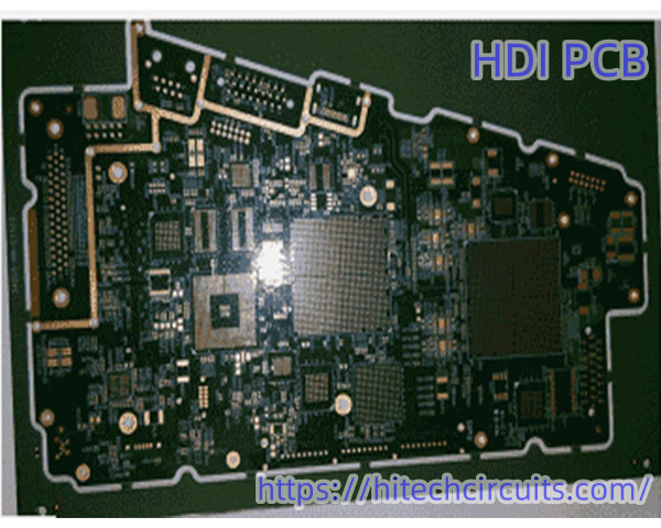
What is HDI PCB?
High-Density Interconnect (HDl) is simply a PCB with more number of interconnections, occupying minimalspace.This results in the miniaturization of the circuit board.The components are placed closer and the boardspace is significantly reduced but the functionality isn't compromised.
To be more precise, a PCB with an average of 120 to 160 pins per square inch is considered as an HDI PCB. The HDl design incorporates dense component placement and versatile routing. The HDl popularized microviatechnology. A denser circuitry is crafted with the implementation of microvias, buried vias, and blind vias. Thedrill to copper is reduced in an HDl design.
What are the advantages of HDI PCBs?
·Phenomenal versatility: HDl boards are ideal where weight, space, reliability, and performance are
primary concerns.
·Compact design:The combination of blind vias, buried vias, and microvias brings down the board space requirement.
·Better signal integrity: HDl incorporates via-in-pad and blind via technology.This helps in placing thecomponents closer to each other which cuts down the signal path length.The HDl technology
removes via stubs and therefore reduces reflections of signal and thus improving signal quality. Ittherefore remarkably improves signal integrity due to shorter signal paths.
·High reliability: The implementation of stacked vias make these boards a super shield against extremeenvironmental conditions.
·Cost-effective:The functionality of a standard 8-layer through-hole board (standard PCB) can be
reduced to a 6-layer HDl board without compromising the quality.
HDl inherently provides a better signal integrity performance than non-HDl because all the stray capacitancesand inductances get reduced when using small blind and buried vias. Since there are no stubs,the impedanceof microvias is close to the trace impedance.The stray capacitance of a normal via is much higher, which causesa greater discontinuity in impedance than a microvia does. Some of the significant differences between the HDI and conventional PCBs are listed below:
|
HDI PCB |
Standard (Through-hole) PCB |
|
Higher component density per square inch |
Lesser compared to HDl |
|
Smaller, lighter boards with more functionality |
Larger and heavier boards |
|
lmplementation of Blind, buried, and microvias Laser direct drilling |
Through-holes |
|
Mechanical drilling |
|
|
Lower number of layers |
Higher number of layers |
|
Compatible with high pin count and low pitch packages |
May face compatibility issues with low pitch packages |
What are the applications of HDI PCBs?
·Healthcare industry--HDI PCB Technology has shown tremendous possibilities in the healthcare and medical fields. For example, tiny, implanted devices such as pacemakers, portable X-Rays and external devices such as hearing aids use the HDI PCB technology.
·Consumer devices--Due to the compact nature, the HDI PCBs are used in most consumer products such as smartphones, tablets, laptop computers, touch screen products and home appliances.
·Aerospace--High Density Interconnect PCB can withstand extreme environmental conditions making it feasible to be utilized in electronics design for missile systems, aircraft, and defense applications.
·Wearables--Due to the size of HDI PCBs, they are widely used in wearable technologies. For example, VR headsets, smartwatches, smart clothing, and more.
Future of HDI PCB Technology
Different kinds of Vias in HDI PCB
Vias are a tiny conductive hole that connects multiple layers in a High Density Interconnect PCB and allows signals to flow through them easily. Depending on the functionality of a PCB, four different types of vias are drilled into an HDI PCB Layout, namely: Through Hole vias, Blind Vias, Buried Vias and Microvias.
Through-Hole Vias – It is a hole pierced using a drill or laser through the HDI PCB from top to bottom connecting all the layers of the multi-layer PCB. The Through-hole PCB is easy to construct and are the most cost-effective type of vias. The Through holes are further divided into Plated Through (with copper pads) Holes and Non-Plated Through Holes (without copper pads).
Blind Vias – A type of via where a hole is pierced using a drill or laser to connect the external layer of multi-layer High Density Interconnect PCB to the internal layer. Since the hole is visible only on one side of the PCB board, it is called Blind via. This type of via is difficult to construct and is expensive.
Buried Vias – A via that connects two internal layers of multi-layer HDI PCB. This via is always inside the printed circuit board and are not visible from the outside. Therefore, it is called buried via. The buried via is also an electroplated hole that needs a separate drill file. The layer count in a buried via is even in number i.e., 2, 4, 6, and on.
Microvias – It is the smallest vias or holes with a diameter less than 150 microns, drilled using a laser. Microvias are most commonly implemented in an HDI PCB Layout Design, usually to connect one layer of the PCB to its adjacent layer and have a very small diameter in comparison to the mechanically drilled vias such as through-hole. Due to their size and ability to connect one layer to an adjacent layer, they enable denser printed circuit boards with more complex designs.
Lamination process and the different types of HDI PCB Layout stack-ups
High Density Interconnect PCB is a multilayer board that are constructed with densely routed layers and the boards are held together through a lamination process. These layers are electrically interconnected using different types of vias. The process of lamination begins with the etching of the inner copper layers. Later they are separated by partially cured laminates and stacked like a book with layers of prepreg on the top and bottom. The HDI PCB stack-up is then pressed and heated enough to liquify the prepreg. These liquified prepregs cool down and stick the layers together. For blind and buried vias stack-ups the HDI PCB Layout will undergo several numbers of sequential laminations. The more the number of laminations, the costlier will be the board. To increase routing density, designers increase the number of layers, producing a complex stack-up. Manufacturers use sequential lamination processes to fabricate such complex designs.
Some of the common types of HDI PCB stack-ups are:
1.HDI PCB (1+N+1): This is the simplest HDI PCB design structure suitable for BGA with lower I/O counts. It has a fine line, microvias and registration technologies capable of 0.4 mm ball pitch, excellent mounting stability and reliability, and may contain copper filled via. It is a qualified material and surface treatment for a Lead-free process. Some of the examples include a Cell phone, UMPC, MP3 Player, PMP, GPS, Memory Card, etc.
2.HDI PCB (2+N+2): This is a moderate complex HDI design structure that contains 2 or more build-up of high-density interconnection layers which allow the conductors on any layer of the PCB to be interconnected freely with copper filled stacked microvias structures. These structures are commonly seen in challenging designs that demand high-level signal transmission performance. They are suitable for BGA with smaller ball pitches and higher I/O counts and can be used to increase routing density in a complicated design while maintaining a thin finished board thickness. Some of the examples include smartphones, PDA, game consoles, and portable video recording devices.
3.Any Layer HDI PCB: This is the most complex HDI PCB design structure where all the layers are high-density interconnection layers which allow the conductors on any layer of the PCB to be interconnected freely with copper filled stacked microvias structures. This structure provides a reliable interconnect solution for highly complex large pin-count devices, such as CPU and GPU chips utilized on handheld and mobile devices while producing superior electrical characteristics. Some of the examples include smartphones, ultra-mobile PC, MP3, GPS, Memory cards, and small electronic devices.
Advantages of HDI PCB
·High Density Interconnect PCB provides designers with the freedom to design and place more components on both sides of the PCB. This is due to the higher wiring density with finer track arrangements on PCBs.
·With the use of microvias and via-in-pad technology, the components in an HDI PCB are densely packed with versatile routing which results in faster transmission of the signal and better signal quality.
·The HDI PCB boards allow you to pack all functions in one board rather than using several boards as in standard PCBs. This results in reducing the size and overall costs compared to the traditional PCBs.
·The HDI PCB boards are highly reliable due to the implementation of stacked vias which make these boards a super shield against extreme environmental conditions. Hence the boards are highly reliable
Laser drilling produces smaller holes and improves the thermal properties of the board.
Using High Density Interconnect PCBs will elevate your technology to a whole new standard. These small PCBs are cost effective, withstand higher frequencies, and are great when used in mobile devices, such as laptops, cell phones, and tablets. Need more advanced information? Then please do not hesitate to contact our us today to learn more about this interesting form of PCB technology. You can send email to Sales3@hitechpcb.com.
https://hitechcircuits.com/pcb-products/high-density-interconnect-pcb/