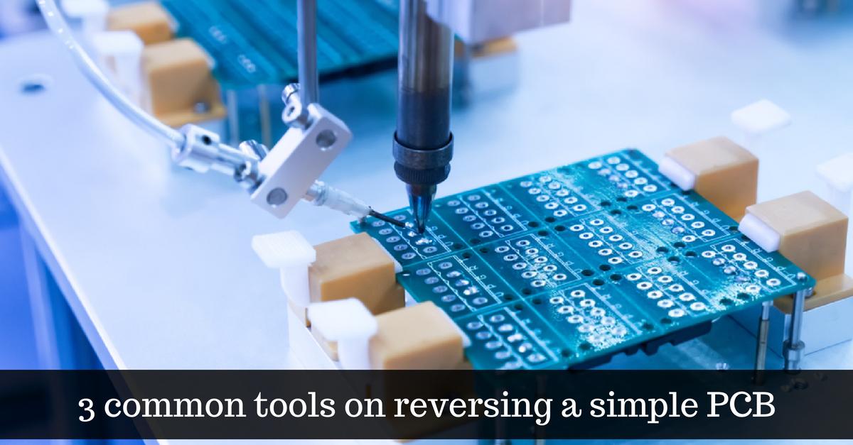
Reverse a Simple PCB Assembly in 3 Common Tools
With the circuit design software, reversing a complex board needs to be familiar. Whenever the reversing works encounter in the electromagnetic compatibility, and interference issues, it also requires to have the hardware circuit background to resolve the possible problems. Moreover, to address these issues, the reverse engineers must have a specific ability. PCB assembly cloning is also known as circuit boards Reverse Engineering.
At this moment for PCB reverse engineering, it is possible to copy any boards theoretically, as long as the copy software can directly open and save the PROTEL PCB file, all placed in the element properties fully supporting PROTEL format, including the placement function.
In this article, we will be talking about reversing a simple PCB assembly in the three common steps that might be useful in creating one.
PCB Assembly Software Copy Board
Software copy board mainly depends on whether the function is complete and is the best to copy all the work that can be done in the software. As a result, higher efficiency includes the placement of components to support PROTEL99SE. Due to the powerful 99SE component library that can download from the Internet directly. Many elements like BGP components have sealed with over hundreds of parts which might, in turn, be too costly to build manually.
To connect with power or ground line, for the stability of the circuits the design would generally have a large copper area. This result in the reduction of circuit noise and interference, due to which it involves the issue of network copper laying.
On the other hand, there is a lot of copper laying to connect while there are many to be isolated for complex circuit boards. However, the copper laying cannot be added correctly if the query is not solved successfully. Therefore, to pave the area for copper, there must be a defining network.
Multi-layer PCB Reversing Engineering
As the middle layer in multi-layer PCB reversing engineering cannot be scanned directly and needs to get milled out to copy multi-layer board, the multi-layer PCB will anyhow get damaged after the reversing work.
Well, fine grinding machine or hand grinding is the current standard method used for multi-layer PCB Reversing Engineering. However, to get into the mid-layers, few PCB assembly requires both ways. As some samples are very fragile and the copper layer could easily get damaged during the process, the procedure requires very experienced technicians to operate.
Appropriate Scanner
The accuracy of the copy board depends on two procedures – Software accuracy and Original image accuracy. It can be said that there is no accuracy limit for the software used for precision 32-bit floating-point representation. As a result, depending on the sharpness of the original scan image is the most important thing.
For instance, taking 1-megapixel photo washable 5-inch photo, and is expected to wash into a 20-inch picture, then the image is unclear. Similarly, for examining the high precision PCB circuit board, it must choose a more upper Dot per Inch (DPI) in the scanning. In other words, the distance between every two points on the scanned image is 1000/DPI in mil. So if the DPI is 400, the distance between two points on the picture is 1000/400 = 2.5 mil, at which the accuracy presently is 2.5mil. The average high intensive induction PCB line width/gap will be over four mils.
With complete proficiency and understanding of PCB Reverse Engineering Process, PCC has a dedicated team of engineers which IPC design specifications and will work on simple to the most complex PCB/PCA projects. Reverse engineering of PCB’s is one of PCC’s specialities, having PCB and PCA knowledge with long years of manufacturing experience, enabled us to provide optimum PCB Reverse Engineering Services.